Which transistor provides more current gain. Transistor
bipolar transistor- an electronic semiconductor device, one of the types of transistors, designed to amplify, generate and convert electrical signals. The transistor is called bipolar, since two types of charge carriers simultaneously participate in the operation of the device - electrons And holes. In this it differs from unipolar(field-effect) transistor, in which only one type of charge carriers participates.
The principle of operation of both types of transistors is similar to the operation of a water valve that regulates the flow of water, only the flow of electrons passes through the transistor. In bipolar transistors, two currents pass through the device - the main "large" current, and the control "small" current. The power of the main current depends on the power of the control. In field-effect transistors, only one current passes through the device, the power of which depends on the electromagnetic field. In this article, we will consider in more detail the operation of a bipolar transistor.
Bipolar transistor device.
The bipolar transistor consists of three semiconductor layers and two PN junctions. PNP and NPN transistors are distinguished by the type of alternating hole and electronic conductivities. It is like two diodes connected face to face or vice versa.

A bipolar transistor has three contacts (electrodes). The contact emerging from the central layer is called base (base). The end electrodes are named collector And emitter (collector And emitter). The base layer is very thin relative to the collector and emitter. In addition to this, the semiconductor regions at the edges of the transistor are not symmetrical. The semiconductor layer on the collector side is slightly thicker than on the emitter side. This is necessary for the correct operation of the transistor.

Consider the physical processes that occur during the operation of a bipolar transistor. Let's take the NPN model as an example. The principle of operation of a PNP transistor is similar, only the voltage polarity between the collector and emitter will be opposite.
As already mentioned in the article on the types of conductivity in semiconductors, in a P-type substance there are positively charged ions - holes. An N-type substance is saturated with negatively charged electrons. In a transistor, the concentration of electrons in the N region is much higher than the concentration of holes in the P region.
Connect a voltage source between the collector and emitter V CE (V CE). Under its action, the electrons from the upper N part will begin to be attracted to the plus and collect near the collector. However, the current cannot flow because the electric field of the voltage source does not reach the emitter. This is prevented by a thick layer of collector semiconductor plus a layer of base semiconductor.

Now we connect the voltage between the base and the emitter V BE , but much lower than V CE (for silicon transistors, the minimum required V BE is 0.6V). Since the layer P is very thin, plus a voltage source connected to the base, will be able to "reach out" with its electric field to the N region of the emitter. Under its action, the electrons will go to the base. Some of them will begin to fill the holes located there (recombine). The other part will not find a free hole for itself, because the concentration of holes in the base is much lower than the concentration of electrons in the emitter.
As a result, the central layer of the base is enriched with free electrons. Most of them will go towards the collector, since the voltage is much higher there. This is also facilitated by a very small thickness of the central layer. Some part of the electrons, although much smaller, will still flow towards the plus of the base.

As a result, we get two currents: a small one - from the base to the emitter I BE, and a large one - from the collector to the emitter I CE.
If the base voltage is increased, then even more electrons will accumulate in the P layer. As a result, the base current will increase slightly, and the collector current will increase significantly. Thus, with a small change in the base current I B , the collector current I varies greatly C. That's how it goes signal amplification in a bipolar transistor. The ratio of the collector current I C to the base current I B is called the current gain. Denoted β , hfe or h21e, depending on the specifics of the calculations carried out with the transistor.
The simplest bipolar transistor amplifier
Let us consider in more detail the principle of signal amplification in the electric plane using the circuit as an example. I will make a reservation in advance that such a scheme is not entirely correct. No one connects a DC voltage source directly to an AC source. But in this case, it will be easier and clearer to understand the amplification mechanism itself using a bipolar transistor. Also, the calculation technique itself in the example below is somewhat simplified.
1. Description of the main elements of the chain
So, let's say we have a transistor with a gain of 200 (β = 200). From the side of the collector, we connect a relatively powerful power source of 20V, due to the energy of which amplification will occur. From the side of the base of the transistor, we connect a weak power source of 2V. To it we connect in series a source of alternating voltage in the form of a sine, with an oscillation amplitude of 0.1V. This will be the signal to be amplified. The resistor Rb near the base is needed in order to limit the current coming from the signal source, which is usually low power.

2. Calculation of base input current I b
Now let's calculate the base current I b. Since we are dealing with alternating voltage, we need to calculate two current values - at maximum voltage (V max) and minimum (V min). Let's call these current values, respectively - I bmax and I bmin.
Also, in order to calculate the base current, you need to know the base-emitter voltage V BE. There is one PN junction between the base and the emitter. It turns out that the base current "meets" a semiconductor diode on its way. The voltage at which a semiconductor diode begins to conduct is about 0.6V. We will not go into details of the current-voltage characteristics of the diode, and for ease of calculation, we will take an approximate model, according to which the voltage across the current-conducting diode is always 0.6V. This means that the voltage between the base and the emitter is V BE = 0.6V. And since the emitter is connected to ground (V E = 0), the voltage from the base to ground is also 0.6V (V B = 0.6V).
Let's calculate I bmax and I bmin using Ohm's law:

2. Calculation of the collector output current I C
Now, knowing the gain (β = 200), we can easily calculate the maximum and minimum values of the collector current (I cmax and I cmin).

3. Calculation of the output voltage V out
The collector current flows through the resistor Rc, which we have already calculated. It remains to substitute the values:
4. Analysis of results
As can be seen from the results, V Cmax turned out to be less than V Cmin . This is because the voltage across V Rc is subtracted from the supply voltage VCC. However, in most cases this does not matter, since we are interested in the variable component of the signal - the amplitude, which increased from 0.1V to 1V. The frequency and sinusoidal waveform have not changed. Of course, a V out / V in ratio of ten times is far from the best indicator for an amplifier, but it is quite suitable for illustrating the amplification process.

So, let's summarize the principle of operation of an amplifier on a bipolar transistor. A current I b flows through the base, carrying a constant and a variable component. The constant component is needed so that the PN junction between the base and the emitter begins to conduct - “opens”. The variable component is, in fact, the signal itself (useful information). The collector-emitter current strength inside the transistor is the result of multiplying the base current by the gain β. In turn, the voltage across the resistor Rc above the collector is the result of multiplying the amplified collector current by the value of the resistor.
Thus, the output V out receives a signal with an increased amplitude of oscillations, but with the preserved shape and frequency. It is important to emphasize that the transistor takes energy for amplification from the VCC power supply. If the supply voltage is not enough, the transistor will not be able to fully work, and the output signal may be distorted.
Operating modes of a bipolar transistor
In accordance with the voltage levels on the electrodes of the transistor, there are four modes of its operation:
- Cut off mode.
- Active mode (active mode).
- Saturation mode.
- Reverse mode.
Cutoff mode
When the base-emitter voltage is lower than 0.6V - 0.7V, the PN junction between base and emitter is closed. In this state, the transistor has no base current. As a result, there will also be no collector current, since there are no free electrons in the base ready to move towards the collector voltage. It turns out that the transistor is, as it were, locked, and they say that it is in cutoff mode.
Active Mode
IN active mode the voltage at the base is sufficient to open the PN junction between the base and the emitter. In this state, the transistor has base and collector currents. The collector current equals the base current multiplied by the gain. That is, the active mode is the normal operating mode of the transistor, which is used for amplification.
Saturation mode
Sometimes the base current may be too large. As a result, the supply power is simply not enough to provide such a collector current that would correspond to the gain of the transistor. In saturation mode, the collector current will be the maximum that the power supply can provide and will not be affected by the base current. In this state, the transistor is not able to amplify the signal, since the collector current does not respond to changes in the base current.
In saturation mode, the transistor conductance is maximum, and it is more suitable for the function of the switch (key) in the "on" state. Likewise, in the cutoff mode, the transistor conductance is minimal, and this corresponds to the switch in the "off" state.
Inverse mode
In this mode, the collector and emitter switch roles: the collector PN junction is forward biased, and the emitter junction is reverse biased. As a result, current flows from the base to the collector. The collector semiconductor region is not symmetrical to the emitter, and the gain in the inverse mode is lower than in the normal active mode. The design of the transistor is made in such a way that it works as efficiently as possible in the active mode. Therefore, in the inverse mode, the transistor is practically not used.
Basic parameters of a bipolar transistor.
current gain- the ratio of the collector current I C to the base current I B . Denoted β , hfe or h21e, depending on the specifics of the calculations carried out with transistors.
β is a constant value for one transistor, and depends on the physical structure of the device. High gain is calculated in hundreds of units, low - in tens. For two separate transistors of the same type, even if they were “neighbors along the pipeline” during production, β may differ slightly. This characteristic of the bipolar transistor is perhaps the most important. If other parameters of the device can often be neglected in the calculations, then the current gain is almost impossible.
Input impedance- resistance in the transistor, which "meets" the base current. Denoted R in (R in). The larger it is, the better for the amplifying characteristics of the device, since there is usually a weak signal source on the base side, from which you need to consume as little current as possible. The ideal option is when the input resistance is equal to infinity.
R in for an average bipolar transistor is several hundred KΩ (kilo-ohm). Here, the bipolar transistor loses very much to the field-effect transistor, where the input resistance reaches hundreds of GΩ (gigaohms).
Output Conductance- the conductivity of the transistor between the collector and emitter. The greater the output conductance, the more collector-emitter current will be able to pass through the transistor at less power.
Also, with an increase in output conductance (or a decrease in output impedance), the maximum load that the amplifier can withstand with little loss in overall gain increases. For example, if a transistor with a low output conductance amplifies a signal 100 times without a load, then when a 1KΩ load is connected, it will already amplify only 50 times. A transistor with the same gain but higher output conductance will have less gain drop. The ideal option is when the output conductivity is equal to infinity (or the output resistance R out \u003d 0 (R out \u003d 0)).
Perhaps today it is difficult to imagine the modern world without transistors, in almost any electronics, from radios and televisions to cars, telephones and computers, one way or another, they are used.
There are two types of transistors: bipolar And field. Bipolar transistors are controlled by current, not voltage. There are powerful and low-power, high-frequency and low-frequency, p-n-p and n-p-n structures ... Transistors are available in different packages and come in different sizes, ranging from SMD chips (in fact, there are much less than a chip) that are designed for surface mounting, ending with very powerful transistors . According to the dissipated power, low-power transistors up to 100 mW, medium power from 0.1 to 1 W and powerful transistors more than 1 W are distinguished.

When talking about transistors, they usually mean bipolar transistors. Bipolar transistors are made from silicon or germanium. They are called bipolar because their work is based on the use of both electrons and holes as charge carriers. Transistors on the circuits are indicated as follows:
One of the extreme regions of the transistor structure is called the emitter. The intermediate region is called the base, and the other extreme is called the collector. These three electrodes form two p-n junctions: between the base and the collector - the collector, and between the base and the emitter - the emitter. Like a conventional switch, a transistor can be in two states - "on" and "off". But this does not mean that they have moving or mechanical parts, they switch from off to on and back using electrical signals.

Transistors are designed to amplify, convert and generate electrical oscillations. The operation of a transistor can be represented by the example of a plumbing system. Imagine a faucet in the bathroom, one transistor electrode is a pipe to the faucet (faucet), the other (second) is a pipe after the faucet, where water flows out, and the third control electrode is just the faucet with which we will turn on the water.
A transistor can be thought of as two diodes connected in series, in the case of NPN the anodes are connected together and in the case of PNP the cathodes are connected.
Distinguish between PNP and NPN transistors, PNP transistors open with negative polarity voltage, NPN with positive polarity. In NPN transistors, the main charge carriers are electrons, and in PNP - holes, which are less mobile, respectively, NPN transistors switch faster.

Uke = collector-emitter voltage
Ube = base-emitter voltage
Ic = collector current
Ib = base current
Depending on the states in which the transitions of the transistor are located, the modes of its operation are distinguished. Since the transistor has two transitions (emitter and collector), and each of them can be in two states: 1) open 2) closed. There are four modes of operation of the transistor. The main mode is the active mode, in which the collector junction is in the closed state, and the emitter junction is in the open state. Transistors operating in the active mode are used in amplifying circuits. In addition to the active, there is an inverse mode, in which the emitter junction is closed and the collector junction is open, a saturation mode, in which both junctions are open, and a cut-off mode, in which both junctions are closed.
When the transistor operates with high-frequency signals, the time of the main processes (the time of movement of carriers from the emitter to the collector) becomes commensurate with the period of change of the input signal. As a result, the ability of a transistor to amplify electrical signals deteriorates with increasing frequency.
Some parameters of bipolar transistors
Constant/pulse voltage collector - emitter.
Constant voltage collector - base.
Constant voltage emitter - base.
Base current transfer ratio limit frequency
Direct/pulse collector current.
Current transfer ratio
Maximum allowable current
Input impedance
Dissipated power.
p-n junction temperature.
Ambient temperature, etc…
Boundary voltage Ukeo gr. is the maximum allowable voltage between collector and emitter, with base open circuit and collector current. The voltage on the collector is less than Ukeo gr. are characteristic of the pulsed operating modes of the transistor at base currents other than zero and the base currents corresponding to them (for n-p-n transistors, the base current> 0, and for p-n-p, on the contrary, Ib<0).
Bipolar transistors can be classified as unijunction transistors, such is, for example, KT117. Such a transistor is a three-electrode semiconductor device with one p-n junction. A unijunction transistor consists of two bases and an emitter.

Recently, composite transistors have often been used in circuits, they are called a pair or Darlington transistors, they have a very high current transfer coefficient, they consist of two or more bipolar transistors, but ready-made transistors are also produced in one package, such is for example TIP140. They turn on with a common collector, if you connect two transistors, they will work as one, the inclusion is shown in the figure below. The use of a load resistor R1 allows you to improve some of the characteristics of the composite transistor.

Some disadvantages of the composite transistor: low performance, especially the transition from open to closed. The forward voltage drop across the base-emitter junction is almost twice that of a conventional transistor. Well, of course, you need more space on the board.
Checking bipolar transistors
Since the transistor consists of two junctions, each of which is a semiconductor diode, you can test the transistor in the same way as you test a diode. The transistor is usually checked with an ohmmeter, both p-n junctions of the transistor are checked: collector - base and emitter - base. To check the direct resistance of the p-n-p transistor junctions, the negative terminal of the ohmmeter is connected to the base, and the positive terminal of the ohmmeter is connected in turn to the collector and emitter. To check the reverse resistance of the transitions, the positive terminal of an ohmmeter is connected to the base. When checking n-p-n transistors, the connection is made the other way around: direct resistance is measured when connected to the base of the positive terminal of the ohmmeter, and reverse resistance is measured when connected to the base of the negative terminal. Transistors can also be called with a digital multimeter in the diode continuity mode. For NPN, we connect the red probe of the device "+" to the base of the transistor, and alternately touch the black probe "-" to the collector and emitter. The device should show some resistance, from about 600 to 1200. Then we change the polarity of connecting the probes, in this case the device should not show anything. For a PNP structure, the order of verification will be reversed.
I want to say a few words about MOSFET transistors (metal-oxide-semiconductor field-effect transistor), (Metal Oxide Semiconductor (MOS)) - these are field-effect transistors, not to be confused with ordinary field-effect transistors! Field-effect transistors have three terminals: G - gate, D - drain, S - source. There are N channel and P, in the designation of these transistors there is a Schottky diode, it passes current from the source to the drain, and limits the drain-to-source voltage.

They are mainly used for switching high currents, they are controlled not by current, like bipolar transistors, but by voltage, and as a rule, they have a very low open channel resistance, the channel resistance is constant and does not depend on current. MOSFET transistors are specially designed for key circuits, it can be said as a relay replacement, but in some cases it can also be amplified, they are used in powerful low-frequency amplifiers.
The advantages of these transistors are as follows:
Minimum drive power and high current gain
Better performance, such as faster switching speed.
Resistant to large voltage impulses.
Circuits using such transistors are usually simpler.
Minuses:
They cost more than bipolar transistors.
Afraid of static electricity.
Most often, N-channel MOSFETs are used for switching power circuits. The control voltage must exceed the threshold of 4V, in general, 10-12V is needed to reliably turn on the MOSFET. The control voltage is the voltage applied between gate and source to turn on the MOSFET.
The values of most transistor parameters depend on the actual operating mode and temperature, and with increasing temperature, the transistor parameters may change. The reference book contains, as a rule, typical (averaged) dependences of transistor parameters on current, voltage, temperature, frequency, etc.
To ensure reliable operation of transistors, it is necessary to take measures that exclude long-term electrical loads close to the maximum permissible ones, for example, it is not worth replacing a transistor with a similar but lower power, this applies not only to power, but also to other parameters of the transistor. In some cases, to increase power, transistors can be connected in parallel, when the emitter is connected to the emitter, the collector to the collector, and the base to the base. Overloads can be caused by various reasons, for example from overvoltage, fast diodes are often used for overvoltage protection.
As for the heating and overheating of transistors, the temperature regime of transistors not only affects the value of the parameters, but also determines the reliability of their operation. You should strive to ensure that the transistor does not overheat during operation; in the output stages of amplifiers, transistors must be placed on large radiators. The protection of transistors from overheating must be ensured not only during operation, but also during soldering. When tinning and soldering, measures should be taken to prevent overheating of the transistor; it is advisable to hold transistors during soldering with tweezers to protect against overheating.
A PNP transistor is an electronic device, in a certain sense, the opposite of an NPN transistor. In this type of transistor design, its PN junctions are opened by reverse polarity voltages with respect to the NPN type. In the device symbol, the arrow, which also defines the emitter terminal, this time points inside the transistor symbol.
Instrument design
The structural diagram of a PNP-type transistor consists of two regions of p-type semiconductor material on either side of an n-type material region, as shown in the figure below.
The arrow defines the emitter and the generally accepted direction of its current ("in" for a PNP transistor).
The PNP transistor has very similar characteristics to its NPN bipolar counterpart, except that the directions of the currents and polarities of the voltages in it are reversed for any of the possible three switching schemes: common base, common emitter and common collector.

The main differences between the two types of bipolar transistors
The main difference between them is that holes are the main current carriers for PNP transistors, NPN transistors have electrons in this capacity. Therefore, the polarities of the voltages feeding the transistor are reversed, and its input current flows from the base. In contrast, with an NPN transistor, the base current flows into it, as shown below in the wiring diagram for both types of devices with a common base and a common emitter.
The principle of operation of the PNP-type transistor is based on the use of a small (like the NPN-type) base current and a negative (unlike the NPN-type) base bias voltage to drive a much larger emitter-collector current. In other words, for a PNP transistor, the emitter is more positive with respect to the base and also with respect to the collector.
Consider the differences of the PNP type in the switching circuit with a common base
Indeed, it can be seen from it that the collector current IC (in the case of an NPN transistor) flows out of the positive pole of the battery B2, passes through the collector terminal, enters into it and must then exit through the base terminal to return to the negative pole of the battery. In the same way, looking at the emitter circuit, you can see how its current from the positive pole of the battery B1 enters the transistor through the base terminal and then penetrates into the emitter.

Thus, both the collector current I C and the emitter current I E pass through the base terminal. Since they circulate in opposite directions in their circuits, the resulting base current is equal to their difference and is very small, since I C is slightly less than I E . But since the latter is still larger, the direction of flow of the differential current (base current) coincides with I E , and therefore the PNP-type bipolar transistor has a current flowing from the base, and an NPN-type bipolar transistor has a current flowing in.
Differences of the PNP type on the example of a switching circuit with a common emitter
In this new circuit, the base-emitter PN junction is turned on by battery voltage B1, and the collector-base junction is reverse-biased by battery voltage B2. The emitter terminal is thus shared between the base and collector circuits.

The total emitter current is given by the sum of the two currents I C and I B ; passing through the output of the emitter in one direction. Thus, we have I E = I C + I B .
In this circuit, the base current I B simply "branches" from the emitter current I E, also coinciding with it in direction. At the same time, a PNP-type transistor still has a current flowing from the base I B, and an NPN-type transistor has a current flowing in.
In the third of the known transistor switching circuits, with a common collector, the situation is exactly the same. Therefore, we do not present it in order to save space and time for readers.
PNP transistor: connection of voltage sources
The voltage source between the base and the emitter (V BE) is connected negative to the base and positive to the emitter, because the operation of the PNP transistor occurs when the base is negatively biased with respect to the emitter.
The emitter supply voltage is also positive with respect to the collector (V CE). Thus, in a PNP-type transistor, the emitter terminal is always more positive with respect to both the base and the collector.
The voltage sources are connected to the PNP transistor as shown in the figure below.

This time the collector is connected to the supply voltage V CC through a load resistor, R L , which limits the maximum current flowing through the device. The base voltage V B , which biases it in the negative direction with respect to the emitter, is applied to it through the resistor R B , which is again used to limit the maximum base current.
Operation of the PNP transistor stage
So, in order to cause base current to flow in a PNP transistor, the base must be more negative than the emitter (current must leave the base) by about 0.7 volts for silicon or 0.3 volts for germanium. The formulas used to calculate the base resistor, base current or collector current are the same as those used for the equivalent NPN transistor and are shown below.

We see that the fundamental difference between an NPN and a PNP transistor is the correct biasing of the pn junctions, since the directions of the currents and the polarity of the voltages in them are always opposite. So for the above circuit: I C = I E - I B since the current must flow from the base.
As a rule, a PNP transistor can be replaced with an NPN transistor in most electronic circuits, the difference is only in the polarity of the voltage and the direction of the current. Such transistors can also be used as switching devices and an example of a PNP switch is shown below.

Transistor characteristics
The output characteristics of a PNP transistor are very similar to those of an equivalent NPN transistor, except that they are rotated 180° to allow for the reversed polarity of voltages and currents (the base and collector currents of the PNP transistor are negative). Similarly, to find the operating points of a PNP transistor, its dynamic load line can be plotted in the 3rd quadrant of the Cartesian coordinate system.
The typical characteristics of the 2N3906 PNP transistor are shown in the figure below.

Transistor pairs in amplifier stages
You may be wondering what is the reason to use PNP transistors when there are many NPN transistors available that can be used as amplifiers or solid state switches? However, the presence of two different types of transistors - NPN and PNP - gives great advantages in the design of power amplifier circuits. These amplifiers use "complementary" or "matched" pairs of transistors (which are one PNP transistor and one NPN connected together as shown in the figure below) in the output stage.

Two corresponding NPN and PNP transistors with close characteristics identical to each other are called complementary. For example, TIP3055 (NPN type) and TIP2955 (PNP type) are good examples of complementary silicon power transistors. They both have a constant current gain β=I C /I B matched within 10% and a high collector current of around 15A, making them ideal for motor control or robotic applications.
In addition, class B amplifiers use matched pairs of transistors in their power output stages as well. In them, the NPN transistor conducts only the positive half-wave of the signal, and the PNP transistor conducts only its negative half.
This allows the amplifier to carry the required power through the loudspeaker in both directions for a given power rating and impedance. As a result, the output current, which is usually on the order of several amperes, is evenly distributed between the two complementary transistors.
Transistor pairs in motor control circuits
They are also used in H-bridge control circuits for reversible DC motors, which make it possible to regulate the current through the motor evenly in both directions of its rotation.
The H-bridge circuit above is so named because the basic configuration of its four transistor switches resembles the letter "H" with the motor in a cross line. The transistor H-bridge is probably one of the most commonly used types of reversible DC motor control circuit. It uses "complementary" pairs of NPN- and PNP-type transistors in each branch, acting as keys in controlling the motor.

Control input A allows the motor to run in one direction, while input B is used for reverse rotation.
For example, when transistor TR1 is on and TR2 is off, input A is connected to the supply voltage (+Vcc), and if transistor TR3 is off and TR4 is on, then input B is connected to 0 volts (GND). Therefore, the motor will rotate in one direction, corresponding to the positive potential of input A and the negative of input B.
If the switch states are changed so that TR1 is off, TR2 is on, TR3 is on, and TR4 is off, the motor current will flow in the opposite direction, causing it to reverse.
By using opposite levels of logic "1" or "0" on inputs A and B, the direction of rotation of the motor can be controlled.
Determining the type of transistors
Any bipolar transistor can be thought of as basically two diodes connected back to back.
We can use this analogy to determine if a transistor is a PNP or NPN type by testing its resistance across its three terminals. Testing each pair of them in both directions with a multimeter, after six measurements we get the following result:
1. Emitter - Base. These pins should act like a normal diode and only conduct current in one direction.
2.Collector - Base. These pins should also act like a normal diode and only conduct current in one direction.
3. Emitter - Collector. These findings should not hold in any direction.
Transition resistance values of both types of transistors
Then we can define the PNP transistor as good and closed. A small output current and a negative voltage at its base (B) with respect to its emitter (E) will open it and allow a much larger emitter-collector current to flow. PNP transistors conduct at a positive emitter potential. In other words, a PNP bipolar transistor will only conduct if the base and collector terminals are negative with respect to the emitter.
Greetings dear friends! Today we will talk about bipolar transistors and the information will be useful primarily for beginners. So, if you are interested in what a transistor is, its principle of operation, and in general what it is eaten with, then we take a comfortable chair and come closer.
Let's continue, and we have content here, it will be more convenient to navigate the article 🙂
Types of transistors
Transistors are mainly of two types: bipolar transistors and field-effect transistors. Of course, it was possible to consider all types of transistors in one article, but I don’t want to cook porridge in your head. Therefore, in this article we will consider exclusively bipolar transistors, and I will talk about field-effect transistors in one of the following articles. We will not interfere with everything in one heap, but we will pay attention to each, individually.
bipolar transistor
The bipolar transistor is a descendant of tube triodes, those that were in TV sets of the 20th century. Triodes went into oblivion and gave way to more functional brothers - transistors, or rather bipolar transistors.
Triodes, with rare exceptions, are used in equipment for music lovers.
Bipolar transistors may look like this.

As you can see, bipolar transistors have three terminals and they can look completely different in design. But on electrical circuits, they look simple and always the same. And all this graphic splendor looks something like this.
 This image of transistors is also called UGO (Conditional graphic designation).
Moreover, bipolar transistors can have a different type of conductivity. There are NPN type and PNP type transistors.
The difference between an n-p-n transistor and a p-n-p transistor is only that it is a "carrier" of electric charge (electrons or "holes"). Those. for a p-n-p transistor, the electrons move from the emitter to the collector and are controlled by the base. For an npn transistor, the electrons go from the collector to the emitter and are controlled by the base. As a result, we come to the conclusion that in order to replace a transistor of one type of conductivity with another in the circuit, it is enough to change the polarity of the applied voltage. Or stupidly change the polarity of the power supply.
Bipolar transistors have three terminals: collector, emitter and base. I think that it will be difficult to get confused by UGO, but in a real transistor it is easy to get confused.
Usually where which output is determined from the directory, but you can simply. The transistor outputs ring like two diodes connected at a common point (in the base region of the transistor).
On the left is a picture for a p-n-p type transistor, when dialing it creates a feeling (through the readings of a multimeter) that you have two diodes in front of you that are connected at one point by their cathodes. For an n-p-n type transistor, the diodes at the base point are connected by their anodes. I think after experimenting with a multimeter it will be more clear.

The principle of operation of a bipolar transistor
And now we will try to figure out how the transistor works. I will not go into details of the internal structure of transistors, as this information only confuses. Better take a look at this picture. 
This image best explains how a transistor works. In this image, a person controls the collector current through a rheostat. He looks at the base current, if the base current increases, then the person also increases the collector current, taking into account the gain of the h21E transistor. If the base current drops, then the collector current will also decrease - the person will correct it with a rheostat.
This analogy has nothing to do with how a transistor actually works, but it makes it easier to understand how it works.
For transistors, rules can be noted that are intended to help facilitate understanding. (These rules are taken from the book).
- The collector is at a more positive potential than the emitter.
- As I said, the base-collector and base-emitter circuits work like diodes.
- Each transistor is characterized by limits such as collector current, base current, and collector-emitter voltage.
- In the event that rules 1-3 are followed, then the collector current Ik is directly proportional to the base current Ib. This ratio can be written as a formula.
![]()
From this formula, you can express the main property of the transistor - a small base current drives a large collector current.
Current Gain.
It is also referred to as
Outcomes from the above, the transistor can operate in four modes:
- Transistor cutoff mode- in this mode, the base-emitter junction is closed, this can happen when the base-emitter voltage is insufficient. As a result, there is no base current and therefore no collector current.
- Transistor active mode is the normal operating mode of the transistor. In this mode, the base-emitter voltage is sufficient to open the base-emitter junction. The base current is sufficient and the collector current is also available. The collector current is equal to the base current multiplied by the gain.
- Transistor saturation mode - the transistor switches to this mode when the base current becomes so large that the power of the power source is simply not enough to further increase the collector current. In this mode, the collector current cannot increase following an increase in the base current.
- Transistor inverted mode- This mode is rarely used. In this mode, the collector and emitter of the transistor are reversed. As a result of such manipulations, the gain of the transistor suffers greatly. The transistor was not originally designed to operate in such a special mode.
To understand how a transistor works, you need to look at specific circuit examples, so let's look at some of them.
Transistor in key mode
The switch-mode transistor is one of the common-emitter transistor circuits. The transistor circuit in the key mode is used very often. This transistor circuit is used, for example, when you need to control a powerful load through a microcontroller. The controller leg is not capable of pulling a powerful load, but the transistor can. It turns out that the controller controls the transistor, and the transistor controls the powerful load. Well, first things first.
The main essence of this mode is that the base current controls the collector current. Moreover, the collector current is much greater than the base current. Here, with the naked eye, you can see that the current amplification of the signal occurs. This amplification is carried out at the expense of the energy of the power supply.
The figure shows a diagram of the operation of a transistor in a key mode.

For transistor circuits, voltages do not play a big role, only currents are important. Therefore, if the ratio of the collector current to the base current is less than the gain of the transistor, then everything is OK.
In this case, even if we have a voltage of 5 volts applied to the base and 500 volts in the collector circuit, then nothing bad will happen, the transistor will dutifully switch the high-voltage load.
The main thing is that these voltages do not exceed the limit values \u200b\u200bfor a particular transistor (set in the characteristics of the transistor).
As far as we know, the current value is a characteristic of the load.
We don't know the resistance of the bulb, but we do know the bulb's operating current is 100mA. In order for the transistor to open and ensure the flow of such a current, you need to select the appropriate base current. We can adjust the base current by changing the value of the base resistor.
Since the minimum value of the transistor gain is 10, the base current must become 10 mA to open the transistor.
 The current we need is known. The voltage across the base resistor will be This value of the voltage across the resistor turned out due to the fact that 0.6V-0.7V is dropped at the base-emitter junction and this must not be forgotten to be taken into account.
As a result, we can quite find the resistance of the resistor
 It remains to choose a specific value from a number of resistors and it's done.
Now you probably think that a transistor switch will work as it should? That when the base resistor is connected to +5 V, the light turns on, when it is turned off, the light goes out? The answer may be yes or it may not.
The thing is that there is a small nuance here.
The light bulb will go out when the potential of the resistor is equal to the ground potential. If the resistor is simply disconnected from the voltage source, then everything is not so simple here. The voltage across the base resistor can miraculously arise as a result of pickups or other otherworldly evil spirits 🙂
To avoid this effect, do the following. Another resistor Rbe is connected between the base and the emitter. This resistor is chosen with a value of at least 10 times the base resistor Rb (In our case, we took a 4.3 kOhm resistor).
When the base is connected to any voltage, the transistor works as it should, the resistor Rbe does not interfere with it. Only a small part of the base current is consumed by this resistor.
In the case when no voltage is applied to the base, the base is pulled up to the ground potential, which saves us from all sorts of interference.
Here, in principle, we figured out the operation of the transistor in the key mode, and as you could see, the key mode of operation is a kind of signal amplification by voltage. After all, with the help of a small voltage of 5V, we controlled a voltage of 12 V.
emitter follower
The emitter follower is a special case of common-collector transistor circuits.

A distinguishing feature of a common collector circuit from a common emitter circuit (transistor switch variant) is that this circuit does not amplify the voltage signal. What went in through the base came out through the emitter, with the same voltage.
Indeed, let's say we applied 10 volts to the base, while we know that at the base-emitter junction, somewhere around 0.6-0.7V is planted. It turns out that the output (at the emitter, at the load Rn) will have a base voltage of minus 0.6V.
It turned out 9.4V, in a word, almost how much came in and out. We made sure that this circuit will not increase the signal to us in terms of voltage.
“What is the point then of turning on the transistor like that?” - you ask. But it turns out that this scheme has another very important property. The common-collector transistor switching circuit amplifies the power signal. Power is the product of current and voltage, but since the voltage does not change, then power increases only due to current! ![]() The load current is the sum of the base current plus the collector current. But if we compare the base current and the collector current, then the base current is very small compared to the collector current. The load current is equal to the collector current. And the result is this formula.
The load current is the sum of the base current plus the collector current. But if we compare the base current and the collector current, then the base current is very small compared to the collector current. The load current is equal to the collector current. And the result is this formula.
Now I think it’s clear what the essence of the emitter follower circuit is, but that’s not all.
The emitter follower has another very valuable quality - high input impedance. This means that this transistor circuit consumes almost no input signal current and places no load on the signal source circuit.
To understand the principle of operation of the transistor, these two transistor circuits will be quite enough. And if you still experiment with a soldering iron in your hands, then insight simply will not keep you waiting, because theory is theory and practice and personal experience are hundreds of times more valuable!
Where to buy transistors?
Like all other radio components, transistors can be bought at any nearest radio parts store. If you live somewhere on the outskirts and have not heard of such stores (as I did before), then the last option remains - order transistors in an online store. I myself often order radio components through online stores, because in an ordinary offline store there may simply not be something.
However, if you are assembling a device purely for yourself, then you can not take a steam bath, but get it from the old one, and, so to speak, breathe new life into the old radio component.
Well friends, that's all for me. Everything I planned to tell you today. If you have any questions, then ask them in the comments, if there are no questions, then write comments anyway, your opinion is always important to me. By the way, do not forget that everyone who leaves a comment for the first time will receive a gift.
Also, be sure to subscribe to new articles, because a lot of interesting and useful things await you further.
I wish you good luck, success and sunny mood!
N/A Vladimir Vasiliev
P.S. Friends, be sure to subscribe to updates! By subscribing you will receive new content directly to your inbox! And by the way, each subscriber will receive a useful gift!
The name of the semiconductor device transistor is formed from two words: transfer - transfer+ resistance - resistance. Because it can really be represented as some kind of resistance, which will be regulated by the voltage of one electrode. A transistor is sometimes also called a semiconductor triode.
The first bipolar transistor was created in 1947, and in 1956 three scientists were awarded the Nobel Prize in Physics for its invention.
A bipolar transistor is a semiconductor device that consists of three semiconductors with an alternating type of impurity conduction. An electrode is connected and led out to each layer. In a bipolar transistor, charges are simultaneously used, the carriers of which are electrons ( n - “negative”) and holes (p - “positive ”), that is, carriers of two types, hence the formation of the prefix of the name “bi” - two.
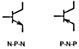
Transistors differ in the type of layer alternation:
P n p -transistor (direct conduction);
Npn- transistor (reverse conduction).
Base (B) is the electrode that is connected to the central layer of the bipolar transistor. The electrodes from the outer layers are called emitter (E) and collector (K).
Figure 1 - The device of a bipolar transistor
The diagrams are labeled " VT ”, in the old Russian-language documentation you can find the designations “T”, “PP” and “PT”. Bipolar transistors are depicted on electrical circuits, depending on the alternation of semiconductor conductivity, as follows:

Figure 2 - Designation of bipolar transistors
In figure 1 above, the difference between collector and emitter is not visible. If you look at the simplified representation of the transistor in the context, you can see that the area p - n The collector junction is greater than that of the emitter.

Figure 3 - Transistor in section
The base is made of a semiconductor with low conductivity, that is, the resistance of the material is high. A prerequisite is a thin base layer for the possibility of a transistor effect. Since the contact area p - n Since the junctions of the collector and emitter are different, then you cannot change the polarity of the connection. This characteristic classifies the transistor as asymmetric devices.
A bipolar transistor has two I-V characteristics (voltage characteristics): input and output.
The input I–V characteristic is the dependence of the base current ( I B ) on the base-emitter voltage ( U BE ).

Figure 4 - Input current-voltage characteristic of a bipolar transistor
The output I–V characteristic is the dependence of the collector current ( I K ) on the collector-emitter voltage ( U KE ).

Figure 5 - Output IV of the transistor
The principle of operation of a bipolar transistor is considered in npn type, for pnp similarly, only holes are considered, not electrons.The transistor has two p-n junctions. In the active mode of operation, one of them is connected with forward bias, and the other with reverse bias. When the EB junction is open, the electrons from the emitter easily move to the base (recombination occurs). But, as mentioned earlier, the base layer is thin and its conductivity is low, so some of the electrons have time to move to the base-collector junction. The electric field helps to overcome (strengthens) the layer transition barrier, since the electrons here are minority carriers. As the base current increases, the emitter-base junction will open more and more electrons will be able to slip from the emitter to the collector. The collector current is proportional to the base current and with a small change in the latter (control), the collector current changes significantly. This is how the signal amplification occurs in a bipolar transistor.

Figure 6 - Active mode of the transistor
Looking at the picture you can explain principle of operation of the transistor a little easier. Imagine that KE is a water pipe and B is a faucet with which you can control the flow of water. That is, the more current you apply to the base, the more you get at the output.
The value of the collector current is almost equal to the emitter current, excluding losses during recombination in the base, which forms the base current, so the formula is valid:
І E \u003d І B + І K.
The main parameters of the transistor:
The current gain is the ratio of the effective value of the collector current to the base current.
Input resistance - following Ohm's law, it will be equal to the ratio of the emitter-base voltage U EB to control current I B .
Voltage amplification factor - the parameter is found by the ratio of the output voltage U EC to input U BE .
The frequency response describes the ability of a transistor to operate up to a certain cut-off frequency of the input signal. After exceeding the limiting frequency, physical processes in the transistor will not have time to occur and its amplifying abilities will be reduced to nothing.
Switching circuits for bipolar transistors
To connect the transistor, only its three outputs (electrodes) are available to us. Therefore, two power supplies are required for its normal operation. One transistor electrode will connect to two sources at the same time. Therefore, there are 3 connection schemes for a bipolar transistor: OE - with a common emitter, OB - a common base, OK - a common collector. Each has both advantages and disadvantages, depending on the application and the required characteristics make the choice of connection.
The switching circuit with a common emitter (CE) is characterized by the greatest amplification of current and voltage, respectively, and power. With this connection, the output AC voltage is shifted by 180 electrical degrees relative to the input. The main disadvantage is the low frequency response, that is, the low value of the cutoff frequency, which makes it impossible to use with a high-frequency input signal.

(OB) provides excellent frequency response. But it does not give such a large voltage signal amplification as with OE. And current amplification does not occur at all, so this circuit is often called a current follower, because it has the property of current stabilization.

The common-collector (CC) circuit has almost the same current gain as the OE circuit, but the voltage gain is almost 1 (slightly less). Voltage offset is not typical for this wiring diagram. I also call it an emitter follower, since the output voltage ( U EB ) correspond to the input voltage.

Application of transistors:
Amplifying circuits;
Signal generators;
Electronic keys.